
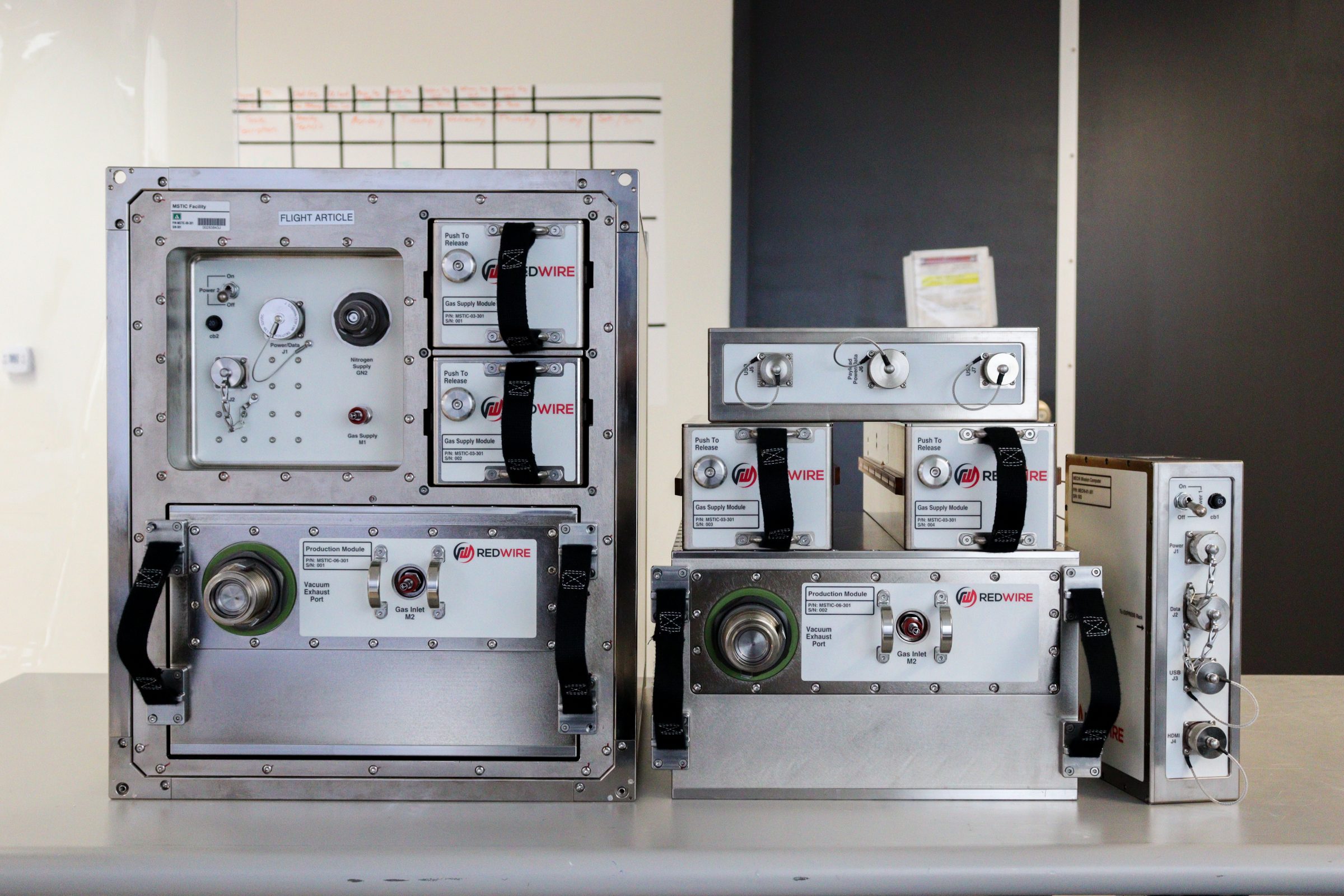
Redwire’s MSTIC facility recently returned to Earth after successfully completing operations on the International Space Station (ISS) for a groundbreaking pathfinder mission to demonstrate advanced in-space manufacturing techniques. Developed in partnership with the ISS National Laboratory and NASA’s In Space Production Applications Flight Demonstrations program, MSTIC is an autonomous semiconductor manufacturing platform that was launched to the ISS onboard Northrop Grumman’s 20th cargo resupply services mission (NG-20) in February 2024.
MSTIC’s mission was an important step in validating space-based manufacturing processes that could deliver superior components beyond what is capable on Earth. This technology could impact industries involved in semiconductor and component manufacturing for use on Earth and in space.
Following successful installation on the ISS, the MSTIC facility completed a series of operations that included manufacturing 18 thin-film semiconductor samples. These samples allowed for the tuning and optimizing of MSTICS’s manufacturing processes in microgravity. The successful flight demo showed that not only was using a scaled down semiconductor production system was possible in microgravity but that there are improvements in the thin-film samples when made in space. MSTIC demonstrated that there is an improvement in the crystal microstructure, which is consistent with what many other researchers have found in various types of crystal growth processes in space.
Learn more about MSTIC and watch the unboxing of the facility after its return to Earth in the video below:
Successful Operations
MSTIC is being developed to 3D print semiconductor devices and thin-film integrated coatings to explore the beneficial effects of microgravity on these structures.
Operations during the first mission demonstrated elements of processing by Physical Vapor Deposition (PVD) and Chemical Vapor Deposition (CVD). MSTIC includes a swappable production vacuum chamber, swappable gas cylinders, a crew serviceable computer, and high-voltage power supplies to produce a fully contained autonomous sputtering system.
The thin film electrical devices are produced using a 3D printed direct write sputtering process at low temperatures and pressures. The process involves both additive and subtractive manufacturing. PVD sputtering acts as an additive process, depositing material on the surface of a substrate, while CVD acts as a subtractive process, cleaning, removing, or milling materials from the substrate surface. Both processes involve plasma-based emitters. The emitter gases can be mixed to accomplish nitriding or reactive sputtering. The CVD gases can be used for cleaning or for condensation in thin film deposition.
Exciting Applications for life on Earth and Beyond
The true potential of MSTIC and manufacturing in space lies in the unique conditions of microgravity. Producing films in microgravity could lead to significantly improved crystal structures, minimizing irregularities often seen in earth-based manufacturing. This could result in films with more uniform thickness, enhanced conductivity, and greater efficiency, ultimately boosting the performance of the devices they’re used in.
Possible applications include improvements to high-temperature and high-frequency devices, power devices, and Ultra-Wide Band Gap and Silicon Carbide sensors. MSTIC could also have immeasurable benefits off-Earth. It could enable on-demand multi-material manufacturing and on-demand manufacturing of electronics in space and on the lunar surface. Developing materials, processes, and manufacturing technologies for on-demand manufacturing capability during deep space exploration missions is critical to successful space operations
MSTIC is just one part of Redwire’s robust portfolio of space biotech and in-space manufacturing capabilities, which spans over 20 facilities developed for the ISS, with 10 currently operating on orbit.
Read more about MSTIC here.


